Application-oriented quantum theory for infrared nitride lasers?
Recently, nitride semiconductor lasers have extended their wavelength reach into the green part of the visible spectrum (emitting at about 530nm in pulsed operation). This has been achieved by using non-standard-orientation gallium nitride (GaN) substrates. The aim in using these substrates has been to reduce or eliminate the strong polarization-induced electric fields that exist in the c-plane orientation of standard GaN substrates. The polarization fields are thought to separate the positive charge carriers (holes) and negative charge carriers (electrons) that should recombine to produce light.
Tarun Sharma and Elias Towe believe that, rather than the polarization field, it is the lattice matching between the InGaN layers and the oriented substrate that determines the longest laser wavelengths achievable in the nitride system [J. Appl. Phys., vol107, p024516, 2010]. Towe is based at Carnegie Mellon University; Sharma is visiting Carnegie Mellon from the Raja Ramanna Centre for Advanced Technology, India.
It is proposed that 'application-oriented nitride substrates' be developed using bulk indium gallium nitride (InGaN) to lattice match the laser epilayers that are needed for longer wavelengths. Sharma and Towe point out that Shuji Nakamura managed to create nitride semiconductor light-emitting diodes emitting red light of 600nm wavelength in 1996. The researchers comment: "We believe it would be possible, by using this concept, to make nitride lasers at the fiber-optic communication windows at 1.3μm and 1.55μm, thus eliminating the need to use the hazardous arsenide/phosphide materials currently used to make communication lasers."
These claims are based on a theoretical analysis of the emission capabilities of quantum wells (QWs) of various thicknesses. In existing technology using GaN templates, the layers that make up the QWs are strained, because the lattice constants of InGaN (a ~ 3.5Å, c ~ 5.7Å) are larger than those of GaN (3.2Å, 5.2Å). As the indium content increases, the strain becomes greater. At higher strains, it becomes difficult to grow high-quality layers of appreciable thickness. Beyond a critical thickness, many defects and dislocations form.
Sharma and Towe note that, from their own experience and that of others, one is limited to strains of less than 3% in constructing InGaAs/GaAs lasers. For InGaN/GaN, this corresponds to indium contents of less than 0.3.
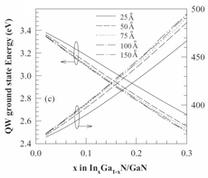
Figure 1: Energy values corresponding to ground-state transitions in InGaN/GaN QWs and corresponding emission wavelength for different values of QW thickness/composition.
On this basis, Sharma and Towe calculate the emission wavelength of InGaN QWs of various thicknesses with GaN barriers with indium content up to 0.3 (Figure 1). The envelope approximation is used with parameters from the literature and adopting a simple formalism for taking account of the change in band structure with strain previously developed by the authors. The calculations do not include polarization fields that can give a red shift of up to 30nm in wavelength. One finds that one is limited to emissions of less than 500nm in wavelength (less than the 520–570nm range for green light).
Although one can shift the upper limit a bit using differently oriented substrates, Sharma and Towe suggest another route to longer wavelengths – using InGaN templates, which they call 'application-oriented nitride substrates' (AONS). This would shift the amount of indium that one could incorporate and hence give longer-wavelength emission. With
In0.1Ga0.9N substrates, one could have wells with indium content up to around 0.4, giving emission up to wavelengths of almost 600nm (orange), they believe. With 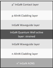
In0.45Ga0.55N substrates, infrared wavelengths of around 1000nm could be accessed.
igure 2: Proposed laser diode structure on InGaN AONS for wide wavelength range. All epilayers are expected to lattice match to AONS except compressively strained QW.
Some InGaN templates are already available, grown on sapphire using hydride vapor phase epitaxy (HVPE). Sharma and Towe believe these could be used to extend the wavelength of light-emitting diodes. For lasers, one would need bulk material. Since ternary indium gallium arsenide (InGaAs) and indium gallium antimonide InGaSb are already available, 'there seems to be no fundamental reason preventing the development of InGaN AONS'. The researchers suggest that a range of AONS to cover extended nitride semiconductor applications could consist of a few products based on 'judicious compromises'. For example, In0.15Ga0.85N substrates could cover the blue, green and red portions of the spectrum.
"Although InGaN AONS do not exist at the present time, it is reasonable to challenge the wafer manufacturers to create them in light of the envisioned numerous device applications that would be enabled by this class of substrates on various orientations," the researchers comment.
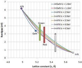
Figure 3: Bandgaps of three nitride ternary alloys (AlGaN, InGaN, and InAlN) vs lattice constant, showing possible bandgaps for InAlN alloy using different bowing parameters (2.5–4.5eV). Measured band bowing can be up to 4.5eV, but 'first principles' calculations suggest its intrinsic value could be about 3eV. Band-bowing values used for AlGaN and InGaN are 1.0eV and 1.2eV, respectively. Vertical blocks show positions for development of nitride LDs at green, red, and infrared wavelengths. Linear interpolation (Vegard's Law) is used to convert from lattice constant to alloy composition.
One major roadblock to this scenario for creating longer-wavelength nitride laser diodes is the cladding that is needed (Figure 2). These layers need to be lattice matched with the underlying substrate and have energy bandgaps that are larger than that of the waveguide layer (unstrained InGaN). One possibility is indium aluminum nitride (InAlN). Unfortunately, the measured bandgaps for this material system are not much different from the corresponding lattice-matched InGaN material (Figure 3). However, it is expected that, as better-quality InAlN is developed, it will have less 'band bowing', leading to a greater difference in bandgap.
http://www.semiconductor-today.com/news_items/2010/FEB/NITRIDELASER_080210.htm
Marcos pinto Dderlee
C.I. 17862728
electronica del estado solido
No hay comentarios:
Publicar un comentario